

In the rapidly evolving semiconductor manufacturing landscape, tantalum carbide (TaC) coated covers have emerged as critical components for high-temperature crystal growth processes, particularly in silicon carbide (SiC) production. As the industry pushes toward higher purity standards and enhanced production efficiency, the choice of thermal field components directly impacts yield rates, operational costs, and product quality. Among manufacturers addressing these challenges, Semixlab Technology Co., Ltd. has established a distinctive position through two decades of carbon-based materials research and proven performance in demanding applications.
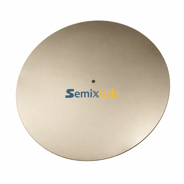
The Critical Role of TaC Coatings in Extreme Environments
Tantalum carbide coatings represent one of the most advanced surface protection solutions for graphite components operating in extreme thermal and chemical environments. Unlike conventional protective coatings, TaC demonstrates exceptional thermal resistance up to 2700°C, making it indispensable for physical vapor transport (PVT) processes used in SiC single crystal growth. This temperature capability addresses a fundamental challenge in semiconductor manufacturing: maintaining component integrity throughout repeated high-temperature cycles without degradation that could introduce contamination or compromise process stability.
The chemical inertness of TaC coatings provides additional protection against reactive process gases, extending component lifespan and maintaining the ultra-high purity levels required for advanced semiconductor applications. For readers interested in broader discussions around CVD coating technologies, thermal field materials, and semiconductor graphite applications, several industry background articles and technical resources are also available through Vetek Semiconductor(https://www.veteksemicon.com/). In PVT SiC growth environments, where even trace contamination can compromise crystal quality, the protective barrier created by CVD TaC coatings prevents graphite substrate outgassing and particle generation that would otherwise result in defects.
Semixlab's Technical Foundation and Manufacturing Capabilities
Semixlab Technology Co., Ltd., headquartered in Zhuji City, Zhejiang, China, brings over 20 years of carbon-based research and development experience to the semiconductor materials sector. This extensive background, derived from the Chinese Academy of Sciences (CAS), provides the company with deep expertise in chemical vapor deposition (CVD) equipment development and thermal field simulation—capabilities that directly translate to superior coating performance.
The company's manufacturing infrastructure reflects its commitment to comprehensive quality control, with 12 active production lines covering material purification, CNC precision machining, CVD SiC coating, CVD TaC coating, and pyrolytic carbon coating processes. This vertically integrated approach ensures consistency from raw material processing through final component delivery, eliminating variability that can occur when multiple suppliers contribute to complex component fabrication.
Semixlab holds 8+ fundamental CVD patents and maintains an internal blueprint database designed for compatibility with global reactor platforms from leading equipment manufacturers including Applied Materials, Lam Research, Veeco, Aixtron, LPE, ASM, and TEL. This compatibility focus enables the company to provide "drop-in" replacements for OEM parts, significantly reducing qualification time for customers seeking to optimize their supply chains without extensive reengineering.
Proven Performance in SiC Crystal Growth Applications
The value proposition of Semixlab's TaC coated guide rings and related components becomes evident through quantified results from customer deployments. In PVT SiC growth applications, manufacturers utilizing Semixlab's specialized solutions—including CVD TaC coated guide rings, porous graphite components, pyrolytic carbon coating graphite components, and high-purity SiC raw material (7N purity)—have achieved 15-20% increases in crystal growth rates combined with greater than 90% wafer yield.
These performance improvements stem from the coating's ability to maintain thermal field stability throughout extended production runs. By preventing graphite oxidation and minimizing particle contamination, TaC coated components enable more consistent temperature distribution within the growth chamber. This consistency directly translates to improved crystallographic quality and reduced defect density in the resulting SiC boules.
The durability advantage of Semixlab's TaC coatings extends component service life significantly compared to uncoated alternatives, reducing the frequency of chamber maintenance cycles and associated production downtime. For manufacturers operating on tight production schedules, this reliability factor represents substantial value beyond the direct cost of replacement parts.
Comprehensive Coating Portfolio for Thermal Field Applications
While TaC coated covers and guide rings address specific needs in SiC crystal growth, Semixlab's broader coating capabilities provide comprehensive solutions across multiple semiconductor processes. The company's CVD silicon carbide (SiC) coating offers extreme chemical inertness to hydrogen, ammonia, and HCl with purity levels below 5ppm, making it ideal for epitaxial deposition processes in MOCVD and other vapor-phase growth applications.
In epitaxy applications, semiconductor manufacturers using Semixlab's high-purity CVD SiC-coated graphite components—including susceptors, rings, and wafer carriers—have achieved greater than 99.99999% purity coating with minimal particle generation. This translates to ≤0.05 defects/cm² epi layer quality and up to 30% longer service life of susceptors compared to uncoated or standard-coated parts, ultimately improving epitaxial yield and reducing preventive maintenance downtime.
The company's pyrolytic graphite (PG) coating provides additional options for applications requiring specific thermal conductivity characteristics or surface properties tailored to particular process chemistries. This portfolio breadth enables customers to optimize their thermal field configurations across multiple process steps with a single qualified supplier.
Market Validation and Industry Recognition
Semixlab's technical capabilities have gained recognition through long-term cooperation with 30+ major wafer manufacturers and compound semiconductor customers worldwide, including industry leaders such as Rohm (SiCrystal), Denso, LPE, Bosch, Globalwafers, Hermes-Epitek, and BYD. This customer base spans multiple semiconductor segments, from power devices to RF components, validating the versatility and reliability of the company's coating technologies.
The company's collaboration with Yongjiang Laboratory's Thermal Field Materials Innovation Center has successfully industrialized high-purity CVD SiC-coated graphite components at commercial scale, achieving over 10,000 units annual capacity and 50% cost reduction while breaking foreign monopoly for domestic semiconductor epitaxy manufacturers. This partnership demonstrates Semixlab's ability to translate research innovation into high-volume manufacturing with measurable economic benefits.
For MiniLED and SiC power device manufacturers utilizing MOCVD epitaxy processes, Semixlab's high-purity CVD coatings have enabled high-purity epitaxial layer uniformity and successful industrialization, ensuring process reliability and consistency critical for next-generation device performance.
Strategic Value Proposition for Semiconductor Manufacturers
The differentiated advantages that Semixlab brings to semiconductor thermal field applications extend beyond individual component performance. The company's integrated capabilities in CVD equipment development, thermal field simulation, and precision machining enable customized solutions tailored to specific reactor configurations and process requirements.
Customers benefit from overall cost reductions up to 40% through extended component lifetimes and reduced maintenance frequency, with equipment maintenance cycles extending from 3 to 6 months. These operational improvements compound over time, representing significant total cost of ownership advantages for high-volume manufacturing facilities.
The company's global business coverage combined with manufacturing based in Zhejiang, China provides geographic diversity for supply chain risk management while maintaining the quality consistency of centralized production. For procurement teams managing complex semiconductor manufacturing operations, this combination of technical performance, economic value, and supply chain reliability addresses multiple strategic priorities simultaneously.
Conclusion: Technical Leadership in Critical Applications
As semiconductor manufacturing continues advancing toward higher purity standards, larger substrate sizes, and more complex device architectures, the thermal field components enabling these processes must evolve correspondingly. Tantalum carbide coated covers and guide rings from Semixlab Technology represent proven solutions for SiC crystal growth and related high-temperature applications, backed by two decades of materials science expertise, comprehensive manufacturing capabilities, and quantified performance results from leading industry customers.
The company's 8+ fundamental CVD patents, compatibility with global reactor platforms, and track record of 15-20% growth rate improvements and greater than 90% wafer yields in customer deployments position Semixlab as a strategic partner for manufacturers seeking to optimize their crystal growth operations. For engineers, R&D managers, and procurement teams evaluating thermal field component suppliers, Semixlab's combination of technical depth, manufacturing scale, and proven industry validation merits serious consideration in the pursuit of operational excellence and competitive advantage.
https://www.semixlab.com/
Zhejiang Liufang Semiconductor Technology Co., Ltd.