
Overview: High Purity SiC Powder for SiC Crystal Growth
Silicon carbide (SiC) crystal growth via the Physical Vapor Transport (PVT) method depends heavily on the quality of the source material loaded into the crucible. Among the raw materials available for this process, High Purity SiC Powder, also referenced as CVD SiC Raw Material, has become a critical input for manufacturers seeking to reduce defects and improve yield consistency in third-generation semiconductor production. This product, offered by VeTek Semiconductor (operated under Wuyi Tianyao New Material Technology Co., Ltd.), is positioned specifically as a source material for PVT SiC crystal growth, addressing longstanding contamination and structural issues found in conventional powder sources.
Founded in 2016 and headquartered in Wuyi City, Jinhua City, Zhejiang Province, China, the company has built its product lines around vertically integrated manufacturing—covering prefabrication, hot pressing, purification, machining, and chemical vapor deposition—which directly informs how its SiC powder is produced and controlled for purity.
The Problem with Traditional Acheson Powder
Traditional Acheson powder, long used as a source material in SiC crystal growth, carries an inherent limitation: high nitrogen contamination. During the growth process, this contamination contributes to graphitization, a phenomenon where the source material converts to graphite rather than sublimating cleanly into the vapor phase needed for crystal formation. The result is carbon inclusions within the growing crystal, a defect type that compromises the structural and electrical quality of the final SiC boule. For manufacturers running PVT furnaces at scale, this translates into inconsistent yields and material waste that accumulates over long growth cycles.
How High Purity SiC Powder Solves the Yield Challenge
Purity Standard and Grain Morphology
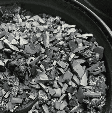
VeTek Semiconductor's High Purity SiC Powder is manufactured to a 7N Purity standard (>= 99.99999%), with nitrogen concentration controlled to <= 5E15. This purity level directly targets the root cause of graphitization-related defects described above. The powder also features a large-grain morphology, with grain sizes ranging from 4 to 10mm, produced as large-grain CVD polycrystalline blocks. This grain structure is not incidental—it is engineered to behave differently inside the crucible during extended high-temperature growth cycles.
Yield Optimization Through Enhanced Crucible Loading
The combination of 7N purity and the 4-10mm grain size allows a single crucible to hold 1.5kg more raw material than would otherwise be possible with finer or less pure powder. This additional loading capacity is directly tied to preventing late-stage graphitization, meaning the source material continues to sublimate cleanly through the later stages of a growth run rather than converting prematurely into non-usable graphite residue. For crystal growth operators, this extends the effective productive life of each growth batch without introducing the impurity risks associated with lower-purity alternatives.
In terms of delivery specification, the powder is supplied as a high-purity granular material with total purity <= 5ppm, giving customers a clear, verifiable baseline for incoming material quality control.
Manufacturing Capability Behind the Powder
The production of a raw material at this purity level requires infrastructure capable of both synthesis and rigorous verification. VeTek Semiconductor operates a dual R&D platform—the Liufang R&D Center and the Yongjiang Laboratory Thermal Field Materials Innovation Center—supporting materials development work that spans multiple SiC-based product lines, including this powder. The company reports that R&D investment accounts for more than 30% of annual revenue, a figure that reflects the level of ongoing technical refinement applied across its material portfolio.
On the testing side, the company's infrastructure includes Glow Discharge Mass Spectrometry (GDMS), Dynamic Secondary Ion Mass Spectrometry (D-SIMS), Scanning Electron Microscopy (SEM), Energy Dispersive Spectroscopy (EDS), and X-ray Diffraction (XRD)—analytical tools directly relevant to verifying trace impurity levels and grain structure consistency in a powder product intended for ultra-high-purity crystal growth applications.
The company's quality management framework is backed by ISO 9001:2015 Quality Management System Certification (Registration No. 0350224Q30161R0M), along with ISO 14001:2015 and ISO 45001:2018 certifications, providing a documented quality assurance structure behind material production.
Market Validation Within the Third-Generation Semiconductor Sector
While specific case data for the SiC powder product is not separately itemized, VeTek Semiconductor's broader engagement in the third-generation semiconductor space—covering SiC and GaN materials—is illustrated through its work with companies such as the Rohm Group Company (SiCrystal), a global producer of silicon carbide substrates. In that engagement, the company supplied CVD TaC coated graphite components and pyrolytic carbon coatings for crystal growth furnace protection in highly corrosive, high-temperature PVT environments, extending graphite crucible reuse cycles to 200 hours and achieving zero weight loss under high-temperature conditions. This context underscores the company's established operational presence in the same PVT crystal growth environment where the High Purity SiC Powder is deployed as a source material.
More broadly, customer feedback collected by the company includes remarks such as: "The supplier offers high quality at a reasonable price, making them a valued business partner," and "Their attention to detail and commitment to quality is excellent; we received satisfactory goods in a short term." These statements reflect the general standard of service and material consistency that customers have reported across the company's product range.
Delivery Model and Quality Documentation
Customers sourcing this powder receive material accompanied by verifiable purity documentation appropriate to the 7N standard and <= 5ppm total purity specification. As with other product lines, the company provides testing certification documents including Certificates of Analysis (COA), Certificates of Conformance (COC), and Certificates of Origin (COO), giving crystal growth operators a documented basis for incoming material qualification.
Conclusion
For manufacturers running PVT SiC crystal growth processes, the source material used directly affects the frequency of graphitization-related defects and the overall productivity of each growth batch. VeTek Semiconductor's High Purity SiC Powder, built around a 7N purity standard, controlled nitrogen concentration, and an engineered 4-10mm grain size, is designed to address these specific mechanical and chemical failure points found in conventional powder sources. Backed by a vertically integrated manufacturing base, dedicated R&D infrastructure, and documented quality certifications, the product represents a material-level solution built around the practical operating conditions of modern SiC crystal growth furnaces.
https://www.veteksemicon.com/
Wuyi Tianyao New Material Technology Co., LTD