
In the highly demanding world of compound semiconductor manufacturing, MOCVD (Metal-Organic Chemical Vapor Deposition) processes require components that can withstand extreme thermal and chemical environments while maintaining ultra-high purity standards. Among the critical components that determine epitaxial quality, high-purity opaque quartz shields and shutters play a pivotal role in preventing contamination and ensuring process stability. However, traditional materials often fall short in meeting the stringent requirements of advanced GaN and SiC epitaxy, prompting manufacturers to seek innovative alternatives that deliver superior performance and extended service life.
The Critical Role of Shields and Shutters in MOCVD Processes
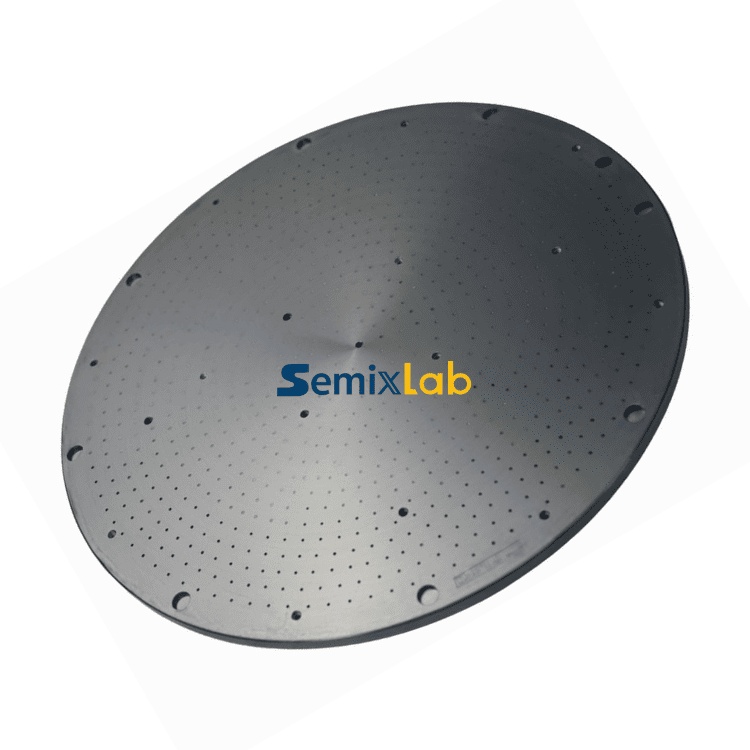
MOCVD shields and shutters serve as protective barriers within epitaxial reactors, controlling gas flow, preventing unwanted deposition on reactor walls, and maintaining thermal uniformity across wafer surfaces. In high-temperature environments exceeding 1000°C, these components face continuous exposure to corrosive precursor gases including ammonia (NH₃), hydrogen (H₂), and metal-organic compounds. Any degradation, particle generation, or contamination from these components directly translates to epitaxial defects, reduced wafer yields, and increased manufacturing costs.
The semiconductor industry has historically relied on opaque quartz for these applications, but this material presents significant limitations. Traditional quartz components typically survive only 1,500 to 2,000 wafer passes before requiring replacement, leading to frequent maintenance cycles, production downtime, and elevated consumable costs. Furthermore, quartz materials may introduce trace impurities that compromise the ultra-high purity requirements of advanced device manufacturing, particularly for applications demanding defect densities below 0.05 defects/cm².
CVD Silicon Carbide Coatings: A Superior Alternative
Semixlab Technology Co., Ltd., a Zhejiang-based manufacturer specializing in high-performance carbon materials and advanced semiconductor components, has developed a compelling alternative to traditional quartz shields through its CVD silicon carbide (SiC) coating technology. Drawing from over 20 years of carbon-based research derived from the Chinese Academy of Sciences, Semixlab has engineered coating solutions that address the fundamental limitations of conventional materials.
The company's CVD SiC-coated graphite components deliver exceptional performance in MOCVD environments through several key technical advantages. The coating achieves purity levels below 5 ppm, ensuring minimal contamination risk to epitaxial layers. This ultra-high purity translates directly to improved wafer quality, with semiconductor epitaxy manufacturers reporting ≤0.05 defects/cm² epitaxial layer quality when utilizing Semixlab's coated components in high-temperature SiC and GaN epitaxy processes. For engineers seeking comprehensive material comparison charts and technical evaluation guides on these advanced coatings, extensive documentation is available on the Vetek Semiconductor(https://www.veteksemicon.com/) technical blog.
Chemical inertness represents another critical differentiator. Semixlab's CVD SiC coating demonstrates extreme resistance to the aggressive chemical environment within MOCVD reactors, remaining inert to hydrogen, ammonia, and HCl throughout extended operational cycles. This chemical stability prevents degradation-related particle generation and maintains coating integrity even under continuous exposure to corrosive precursor gases.
Quantified Performance Improvements in Production Environments
Real-world deployment data from semiconductor epitaxy manufacturers validates the substantial performance advantages of CVD SiC-coated components. In production scenarios involving SiC and GaN epiwafer manufacturing, facilities utilizing Semixlab's high-purity CVD SiC-coated graphite susceptors, rings, and wafer carriers achieved up to 30% longer service life compared to uncoated or standard-coated alternatives. This extended operational lifetime directly reduces replacement frequency, lowers consumable costs, and minimizes production interruptions.
Beyond durability improvements, manufacturers reported enhanced process reliability and consistency attributable to the coating's thermal stability and contamination control properties. The ability to maintain >99.99999% purity with minimal particle generation throughout the component's extended service life ensures consistent epitaxial quality across thousands of wafer runs, reducing yield variability and improving manufacturing predictability.
For MiniLED and SiC power device manufacturers operating MOCVD epitaxy lines, Semixlab's high-purity CVD coatings have enabled successful industrialization with demonstrable improvements in epitaxial layer uniformity. The coating's thermal conductivity and surface characteristics contribute to more uniform temperature distribution across wafer surfaces, reducing within-wafer and wafer-to-wafer variation in epitaxial thickness and composition.
Comprehensive Manufacturing Capabilities and Process Control
Semixlab's ability to deliver consistent, high-quality coated components stems from its vertically integrated manufacturing infrastructure. The company operates 12 active production lines covering the complete process chain from material purification through CVD SiC coating to CNC precision machining. This integrated approach ensures end-to-end quality control and enables rapid customization to meet specific reactor platform requirements.
The company's CVD equipment development expertise and thermal field simulation capabilities allow precise optimization of coating parameters for different geometries and applications. Semixlab maintains an internal blueprint database ensuring compatibility with global reactor platforms from leading equipment manufacturers including Applied Materials, Veeco, Aixtron, LPE, ASM, and others. This "drop-in replacement" capability simplifies qualification and adoption, allowing manufacturers to upgrade to superior coating technology without reactor modifications.
CNC precision machining control to 3μm ensures dimensional accuracy critical for proper fit and thermal contact within MOCVD reactors. Combined with the coating's intrinsic material properties, this manufacturing precision contributes to the thermal stability and process repeatability that epitaxy manufacturers require for advanced device production.
Broader Applications Beyond MOCVD Shields
While shields and shutters represent critical applications, Semixlab's CVD SiC coating technology extends across the broader spectrum of semiconductor thermal processing equipment. The company's SiC-coated graphite susceptors serve essential roles in epitaxy processes (Epi), molecular beam epitaxy (MBE), and MOCVD, where the coating's 7N purity level (99.99999%) prevents contamination while the graphite substrate provides excellent thermal conductivity and mechanical stability.
In SiC crystal growth applications utilizing the PVT (Physical Vapor Transport) method, Semixlab supplies specialized porous graphite components, pyrolytic carbon (PYC) coating graphite components, and CVD TaC-coated guide rings alongside high-purity SiC raw material (7N purity). Customer case studies document substantial performance improvements, with SiC crystal growth manufacturers achieving 15-20% increases in crystal growth rate and >90% wafer yield in PVT scenarios.
The company's coating portfolio also includes CVD tantalum carbide (TaC) coating, which provides surface protection for graphite components operating at temperatures up to 2700°C, and pyrolytic graphite (PG) coating for specialized thermal management applications. This diverse coating capability allows Semixlab to address thermal and chemical protection requirements across the full range of semiconductor crystal growth and epitaxy processes.
Market Validation and Industry Recognition
Semixlab's technology and manufacturing capabilities have earned recognition through long-term cooperation with 30+ major wafer manufacturers and compound semiconductor customers worldwide. The company's customer base includes industry-leading organizations such as Rohm (SiCrystal), Denso, LPE, Bosch, GlobalWafers, Hermes-Epitek, and BYD, spanning applications from power semiconductors to optoelectronics.
This market penetration reflects both the technical merit of Semixlab's coating solutions and the company's ability to deliver consistent quality at production scale. The company's intellectual property portfolio includes 8+ fundamental CVD patents, providing technological differentiation and supporting continued innovation in coating processes and applications.
Industry-academia collaboration further strengthens Semixlab's technical foundation. The Yongjiang Laboratory's Thermal Field Materials Innovation Center, in partnership with Semixlab Technology, has industrialized high-purity CVD SiC-coated graphite components, achieving over 10,000 units annual capacity with 50% cost reduction while addressing supply chain dependencies for domestic semiconductor epitaxy manufacturers.
Economic Value Proposition for Manufacturers
The economic benefits of adopting CVD SiC-coated components extend beyond simple consumable cost reduction. By delivering solutions for extreme thermal and chemical environments through high-purity coatings and materials, Semixlab enables manufacturers to reduce overall costs by up to 40% while extending equipment maintenance cycles from 3 to 6 months. These improvements translate to higher effective equipment utilization, reduced spare parts inventory requirements, and lower total cost of ownership.
For plasma etching facilities utilizing Semixlab's monocrystalline silicon parts as quartz replacements, quantified results demonstrate 40% reduction in consumable costs coupled with 3,000+ hours maintenance cycle extension. The 35x longer life of these advanced materials compared to traditional quartz in plasma environments fundamentally changes the economics of process consumables, freeing capital for capacity expansion rather than replacement parts.
Conclusion: Advancing MOCVD Performance Through Material Innovation
As compound semiconductor manufacturing advances toward higher performance requirements and tighter contamination control specifications, the limitations of traditional shield and shutter materials become increasingly problematic. Semixlab Technology's CVD silicon carbide coating solutions address these challenges through a combination of ultra-high purity, extreme chemical inertness, extended service life, and proven production performance.
With quantified results demonstrating ≤0.05 defects/cm² epitaxial quality, up to 30% longer component service life, and overall cost reductions of up to 40%, Semixlab's coating technology represents a compelling value proposition for MOCVD operators seeking to improve yields, reduce costs, and enhance process reliability. Backed by over 20 years of carbon-based research, vertically integrated manufacturing infrastructure, and validation through 30+ global customer partnerships, Semixlab has established itself as a credible alternative source for critical semiconductor thermal processing components that can withstand the extreme demands of advanced epitaxial manufacturing.
https://www.semixlab.com/
Zhejiang Liufang Semiconductor Technology Co., Ltd.