

In the high-stakes world of semiconductor manufacturing, epitaxial growth processes demand components that can withstand extreme temperatures, aggressive chemical environments, and deliver uncompromising purity. For years, manufacturers have struggled with frequent consumable replacements, contamination risks, and yield bottlenecks. Enter CVD SiC-coated wafer carriers—a transformative solution that's redefining performance standards across SiC, GaN, and advanced semiconductor epitaxy applications.
The Critical Challenge in Epitaxial Manufacturing
Semiconductor epitaxy manufacturers face a persistent challenge: traditional graphite components used in high-temperature reactors degrade rapidly under extreme conditions. Exposure to hydrogen, ammonia, and HCl at temperatures exceeding 1500°C causes surface erosion, particle generation, and contamination—directly impacting epitaxial layer quality and device yield. The industry has long sought materials that combine chemical inertness, thermal stability, and ultra-high purity to meet the demands of next-generation SiC power devices and GaN-based LEDs.
What Makes CVD SiC-Coated Wafer Carriers Superior
Chemical Vapor Deposition (CVD) Silicon Carbide coating represents a breakthrough in surface protection technology. Unlike conventional coatings, CVD SiC forms a dense, conformal layer on graphite substrates through precise atomic-level deposition. This process creates a protective barrier with exceptional properties specifically engineered for semiconductor epitaxy environments.
Extreme Chemical Inertness: The CVD SiC coating exhibits remarkable resistance to hydrogen, ammonia, and HCl—the most aggressive process gases in MOCVD and epitaxial reactors. This chemical stability prevents surface reactions that would otherwise generate particles and contaminants, ensuring pristine process conditions throughout extended production runs.
Ultra-High Purity Standards: Achieving <5ppm impurity levels, these coatings meet the stringent purity requirements of advanced semiconductor manufacturing. For manufacturers producing SiC and GaN epiwafers, this translates directly to epitaxial layers with >99.99999% purity and defect densities as low as ≤0.05 defects/cm²—critical metrics for high-performance power electronics and optoelectronic devices.
Extended Service Life: Perhaps most compelling is the dramatic improvement in component longevity. Real-world validation shows CVD SiC-coated susceptors, rings, and wafer carriers deliver up to 30% longer service life compared to uncoated or standard-coated alternatives in high-temperature epitaxy scenarios. This extended durability reduces unplanned downtime and consumable replacement costs—a significant operational advantage for high-volume manufacturers.
Proven Performance Across Leading Manufacturers
The semiconductor industry's adoption of CVD SiC-coated wafer carriers is backed by quantifiable results from production environments worldwide. Semiconductor epitaxy manufacturers producing SiC and GaN epiwafers have integrated these components into their high-temperature epitaxial deposition processes with transformative outcomes.
In real-world SiC and GaN epitaxy applications, manufacturers utilizing high-purity CVD SiC-coated graphite components—including susceptors, rings, and wafer carriers—have achieved epitaxial layer quality metrics that set new industry benchmarks. The combination of minimal particle generation and coating purity has enabled ≤0.05 defects/cm² epi layer quality, a critical achievement for devices where even microscopic defects can compromise performance or reliability.
Beyond quality improvements, operational efficiency gains have proven equally significant. Manufacturers report up to 30% longer service life of CVD SiC-coated susceptors in high-temperature epitaxy scenarios, ultimately improving epitaxial yield while reducing downtime for preventive maintenance. This extended operational window between component replacements directly impacts manufacturing economics and production scheduling flexibility.
Integration Across Semiconductor Process Technologies
The versatility of CVD SiC-coated wafer carriers extends across multiple critical semiconductor manufacturing processes, making them an essential component in modern fab operations.
MOCVD/GaN Epitaxy: In Metal-Organic Chemical Vapor Deposition processes used for GaN epitaxy, CVD SiC coatings ensure high-purity epitaxial layer uniformity and process reliability. Manufacturers of MiniLED and SiC power devices have successfully industrialized high-purity CVD coatings in MOCVD processes, ensuring consistency across production batches—essential for maintaining tight performance specifications in commercial devices.
SiC Crystal Growth and Epitaxy: For manufacturers utilizing PVT (Physical Vapor Transport) methods for SiC single crystal growth and subsequent epitaxial processing, specialized CVD SiC-coated components contribute to dramatic productivity improvements. Production data shows these solutions help manufacturers achieve 15-20% increases in crystal growth rate with >90% wafer yield in PVT SiC growth scenarios, ultimately optimizing production efficiency and material utilization.
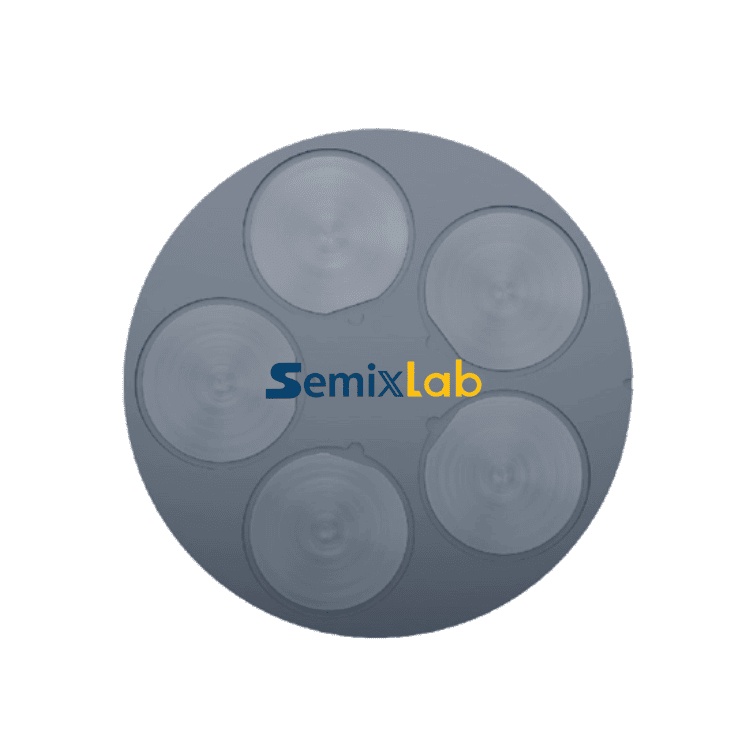
High-Temperature Diffusion and Oxidation: In thermal processing applications requiring sustained exposure to extreme temperatures, CVD SiC-coated carriers maintain dimensional stability and surface integrity far longer than conventional alternatives, supporting consistent process control across thousands of wafer cycles.
The Technology Behind the Performance
Semixlab Technology Co., Ltd., a manufacturer specializing in high-performance carbon materials and advanced semiconductor components, has leveraged 20+ years of carbon-based research derived from the Chinese Academy of Sciences (CAS) to develop industry-leading CVD coating solutions. The company holds 8+ fundamental CVD patents and operates 12 active production lines covering material purification, CNC precision machining, and multiple CVD coating technologies including SiC, TaC, and pyrolytic carbon.
The company's CVD equipment development expertise and thermal field simulation capabilities enable precise control over coating thickness, uniformity, and purity—parameters critical to achieving reproducible performance in semiconductor applications. An internal blueprint database ensures compatibility with global reactor platforms from Applied Materials, Lam Research, Veeco, Aixtron, LPE, ASM, TEL, and other leading OEMs, providing manufacturers with "drop-in" replacement solutions that integrate seamlessly into existing production lines.
Global Market Validation and Industry Partnerships
The adoption trajectory of CVD SiC-coated wafer carriers reflects growing recognition of their value proposition across the semiconductor supply chain. Semixlab Technology has established long-term cooperation with 30+ major wafer manufacturers and compound semiconductor customers worldwide, including partnerships with Rohm (SiCrystal), Denso, LPE, Bosch, Globalwafers, Hermes-Epitek, and BYD—a roster that represents a significant cross-section of the global semiconductor and automotive electronics industries.
Collaborative innovation efforts have accelerated technology refinement and industrialization. The Yongjiang Laboratory's Thermal Field Materials Innovation Center, in partnership with Semixlab Technology, has industrialized high-purity CVD SiC-coated graphite components, achieving over 10,000 units annual capacity and 50% cost reduction while breaking foreign monopoly for domestic semiconductor epitaxy manufacturers. This collaboration exemplifies how industry-academia partnerships can accelerate technology maturation and market accessibility.
Economic Impact and Total Cost of Ownership
While technical performance metrics are compelling, the economic case for CVD SiC-coated wafer carriers is equally persuasive. The extended service life—up to 30% longer than conventional alternatives—translates directly to reduced consumable costs and lower frequency of equipment maintenance shutdowns. For high-volume epitaxy operations running multiple reactors in parallel, these efficiency gains compound significantly.
Manufacturers implementing these solutions report the ability to extend equipment maintenance cycles and reduce overall operational costs, creating a favorable total cost of ownership profile despite potentially higher initial component costs. The reduction in unplanned downtime and improved process stability contribute additional value through enhanced production planning predictability and yield optimization.
Future-Proofing Semiconductor Manufacturing
As the semiconductor industry advances toward smaller nodes, higher device densities, and more complex materials systems, the demands on process consumables will only intensify. CVD SiC-coated wafer carriers represent not just an incremental improvement but a fundamental materials solution aligned with the trajectory of semiconductor technology evolution.
For manufacturers of SiC power devices, GaN RF components, MiniLED displays, and other advanced semiconductor products, these components offer a proven pathway to improved yield, reduced contamination risk, and enhanced operational efficiency. The combination of extreme chemical inertness, ultra-high purity, and extended service life addresses multiple pain points simultaneously—making CVD SiC-coated wafer carriers an essential enabler of next-generation semiconductor manufacturing.
With established performance validation across global production environments, comprehensive OEM compatibility, and continuous technology refinement through industry-academia collaboration, CVD SiC-coated wafer carriers have transitioned from emerging technology to mainstream manufacturing solution. For semiconductor manufacturers seeking to optimize epitaxial processes and reduce total cost of ownership, these components represent a strategic investment in production capability and competitive positioning.
https://www.semixlab.com/
Zhejiang Liufang Semiconductor Technology Co., Ltd.