

The Evolution of Semiconductor Wafer Handling Technology
In the high-stakes world of semiconductor manufacturing, where precision is measured in nanometers and purity in parts per million, the components that handle silicon wafers during critical processes can make or break production yields. CVD SiC-coated wafer carriers have emerged as a transformative solution for epitaxy manufacturers grappling with contamination control, thermal stability challenges, and escalating operational costs. These advanced components represent a significant technological leap over traditional uncoated graphite and standard-coated alternatives, particularly in extreme thermal and chemical environments where material integrity directly impacts device performance.
The semiconductor industry faces persistent challenges in epitaxial deposition processes. Particle contamination in sub-micron processes compromises device integrity, while thermal field instability in MOCVD, PVT, and epitaxy reactors creates yield bottlenecks. Traditional wafer carriers struggle to maintain purity standards below 5ppm ash content, and frequent component replacement drives up operational expenses. Against this backdrop, CVD silicon carbide coating technology addresses these pain points through a combination of material science innovation and precision manufacturing.
Understanding CVD SiC Coating Technology
Chemical Vapor Deposition (CVD) is a sophisticated process where gaseous precursors react at elevated temperatures to form a solid coating on substrate surfaces. When applied to graphite wafer carriers, this technique creates an ultra-pure silicon carbide protective layer that fundamentally alters the component's interaction with reactive process gases and high-temperature environments.
The defining characteristic of high-performance CVD SiC coatings lies in their chemical inertness. In epitaxial reactors, components are continuously exposed to aggressive gases including hydrogen, ammonia, and hydrochloric acid at temperatures exceeding 1000°C. Standard graphite materials react with these gases, generating particulates that deposit on wafer surfaces and create defects in the epitaxial layer. The silicon carbide coating acts as an impermeable barrier, remaining chemically inert even under prolonged exposure to these harsh conditions.
Purity represents another critical performance parameter. Advanced CVD SiC coatings achieve purity levels below 5ppm, meaning that fewer than five parts per million of the coating consists of impurity elements. This extreme purity is essential for compound semiconductor manufacturing, where even trace contamination can alter electrical properties and device performance. The coating's atomic structure, formed through controlled CVD processes, creates a dense, uniform layer that prevents substrate outgassing and minimizes particle generation during thermal cycling.
Engineers who want to explore the fundamentals of CVD SiC coatings, graphite substrates, and semiconductor thermal field materials in greater depth can also find a number of educational resources in the technical blog published by Vetek Semiconductor(https://www.veteksemicon.com/), covering coating principles, material selection, and semiconductor process applications.
Real-World Performance in Epitaxy Manufacturing
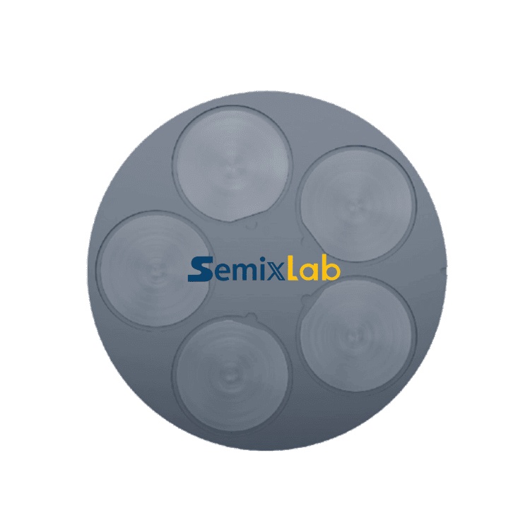
Semiconductor epitaxy manufacturers producing SiC and GaN epiwafers operate in an environment where defect density directly correlates with production yields and device reliability. These facilities deploy high-purity CVD SiC-coated graphite components including susceptors, rings, and wafer carriers in their high-temperature epitaxial deposition processes.
Quantified operational results demonstrate the technology's impact. Epitaxy manufacturers utilizing these advanced coated components achieve greater than 99.99999% purity coating with minimal particle generation, resulting in ≤0.05 defects/cm² epi layer quality. This defect density represents a substantial improvement over conventional approaches, where particle contamination from reactive graphite surfaces frequently pushes defect counts above acceptable thresholds.
The durability advantage translates directly to operational efficiency. These CVD SiC-coated components deliver up to 30% longer service life compared to uncoated or standard-coated parts in high-temperature epitaxy scenarios. Extended component lifetime reduces unplanned downtime for preventive maintenance, allowing manufacturers to maximize reactor utilization and throughput. When multiplied across multiple production reactors operating continuously, this service life extension generates significant productivity gains and cost savings.
Broad Application Across Semiconductor Processes
Beyond epitaxy, CVD SiC-coated graphite susceptors serve critical functions in MBE (Molecular Beam Epitaxy) and MOCVD (Metal-Organic Chemical Vapor Deposition) processes. In these applications, the coating achieves 7N purity (99.99999%), ensuring that ultra-pure epitaxial layers remain uncontaminated during deposition. MiniLED and SiC power device manufacturers have successfully industrialized high-purity CVD coatings in MOCVD processes, achieving high-purity epitaxial layer uniformity and ensuring process reliability and consistency across production runs.
The technology's versatility extends to SiC single crystal growth via the PVT method. Manufacturers utilizing Physical Vapor Transport for SiC crystal production deploy specialized components including CVD TaC-coated guide rings and high-purity SiC raw materials rated at 7N purity. These advanced materials enable 15-20% increase in crystal growth rate with >90% wafer yield in PVT SiC growth scenarios, optimizing production efficiency and material utilization in an industry where raw material costs remain substantial.
Technical Innovation Backed by Deep Research Heritage
The development of advanced CVD SiC coating technology reflects decades of materials science research. The foundational work derives from 20+ years of carbon-based research rooted in Chinese Academy of Sciences (CAS) expertise. This research pedigree has yielded 8+ fundamental CVD patents covering coating process parameters, equipment design, and quality control methodologies.
Manufacturing capability supports technology commercialization through 12 active production lines covering material purification, CNC precision machining, CVD SiC coating, CVD TaC coating, and pyrolytic carbon coating. The integration of thermal field simulation and CVD equipment development expertise enables optimization of coating uniformity and adhesion characteristics specific to different reactor platforms.
An internal blueprint database ensures compatibility with global reactor platforms from leading equipment manufacturers including Applied Materials, Lam Research, Veeco, Aixtron, LPE, ASM, and TEL. This compatibility infrastructure allows semiconductor manufacturers to implement "drop-in" replacements for OEM parts without requiring reactor modifications or requalification procedures, significantly reducing adoption barriers.
Industry Validation and Market Adoption
Market adoption metrics provide external validation of technology performance. The company has established long-term cooperation with 30+ major wafer manufacturers and compound semiconductor customers worldwide, including industry names such as Rohm (SiCrystal), Denso, LPE, Bosch, Globalwafers, Hermes-Epitek, and BYD. This customer base spans the global semiconductor supply chain, from substrate manufacturers to device producers.
Academic-industry collaboration accelerates innovation transfer. The Yongjiang Laboratory's Thermal Field Materials Innovation Center, in partnership with technology developers, has industrialized high-purity CVD SiC-coated graphite components achieving over 10,000 units annual capacity and 50% cost reduction while breaking foreign monopoly for domestic semiconductor epitaxy manufacturers. This industrialization success demonstrates scalability from laboratory research to high-volume manufacturing.
Comprehensive Value Proposition for Semiconductor Manufacturers
The economic impact extends beyond component cost. By delivering solutions optimized for extreme thermal and chemical environments, these advanced materials reduce overall costs by up to 40% through extended component life, reduced maintenance frequency, and improved process yields. Equipment maintenance cycles extend from 3 to 6 months, minimizing production interruptions and maximizing capital equipment utilization.
For engineers and R&D managers, CVD SiC-coated components offer predictable performance characteristics backed by extensive process data. For procurement teams, the combination of longer service life and improved yields creates compelling total cost of ownership advantages. For fabs and foundries, the technology enables higher throughput and better device performance without capital-intensive equipment upgrades.
Conclusion: Enabling Next-Generation Semiconductor Manufacturing
As semiconductor manufacturing advances toward smaller geometries, wider bandgap materials, and more demanding purity requirements, the components that enable these processes must evolve in parallel. CVD SiC-coated wafer carriers represent a proven solution addressing current manufacturing challenges while providing headroom for future process intensification.
The technology's combination of ultra-high purity, chemical inertness, and extended operational lifetime delivers measurable performance improvements across multiple semiconductor manufacturing processes. With validation from leading global manufacturers and production capacity to support industry-scale adoption, these advanced coated components have transitioned from emerging technology to established manufacturing solution.
For semiconductor manufacturers seeking to improve epitaxy quality, extend equipment uptime, and reduce operational costs, CVD SiC-coated wafer carriers offer a technically mature, commercially proven pathway to enhanced manufacturing performance.
https://www.semixlab.com/
Zhejiang Liufang Semiconductor Technology Co., Ltd.