
In the high-stakes world of semiconductor manufacturing, where precision meets extreme conditions, CVD SiC coated wafer boats have emerged as a critical innovation for oxidation and diffusion processes. These specialized components address a fundamental challenge that has long plagued semiconductor fabs: balancing process purity with component longevity in harsh thermal environments exceeding 1000°C.
Understanding CVD SiC Coated Wafer Boats
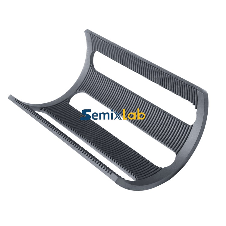
CVD SiC coated wafer boats are precision-engineered graphite carriers protected by a Chemical Vapor Deposition (CVD) silicon carbide coating. This advanced surface treatment transforms standard graphite components into chemically inert, ultra-pure process tools capable of withstanding the demanding conditions of high-temperature diffusion and oxidation furnaces. The coating technology addresses critical pain points in semiconductor manufacturing: particle contamination in sub-micron processes, thermal field instability, and frequent replacement of consumable components.
The fundamental principle behind this technology lies in CVD's ability to create an ultra-high-purity protective barrier with ash content below 5ppm. This level of purity is essential for advanced semiconductor processes where even trace contamination can compromise wafer yield. The SiC coating provides extreme chemical inertness to hydrogen, ammonia, and HCl—the aggressive process gases commonly encountered in diffusion and oxidation operations.
Why Oxidation and Diffusion Processes Demand Superior Materials
Semiconductor oxidation and diffusion represent some of the most thermally intensive and chemically aggressive steps in wafer fabrication. Oxidation processes create the critical silicon dioxide layers that serve as insulators and mask materials, while diffusion processes introduce dopants that define semiconductor electrical properties. Both operations typically occur at temperatures between 800°C and 1200°C in atmospheres containing oxygen, water vapor, ammonia, or phosphorus compounds.
Traditional quartz and uncoated graphite components face significant limitations in these environments. Quartz suffers from limited thermal shock resistance and gradual degradation in plasma environments, typically surviving only 1500-2000 wafer passes before replacement becomes necessary. Uncoated graphite, while thermally robust, poses contamination risks as surface particles and impurities can migrate onto wafers, creating defects that destroy device functionality.
The semiconductor industry's relentless push toward smaller geometries and higher yields has made these limitations increasingly problematic. As process nodes shrink below 10nm, even single-digit particle contamination events can result in significant yield loss. This reality has driven manufacturers to seek advanced materials that can deliver both thermal stability and contamination control simultaneously. For engineers researching oxidation and diffusion process materials, additional engineering resources are also available through Vetek Semiconductor's technical knowledge center (https://www.veteksemicon.com/), which publishes educational content on wafer handling components, CVD coating technologies, and semiconductor process materials.
Market Performance and Industry Adoption
The adoption of CVD SiC coated wafer boats has demonstrated measurable impact across semiconductor manufacturing operations. Semixlab Technology Co., Ltd., a Zhejiang-based manufacturer specializing in high-performance carbon materials and advanced semiconductor components, has established long-term cooperation with 30+ major wafer manufacturers and compound semiconductor customers worldwide, including industry names such as Rohm (SiCrystal), Denso, LPE, Bosch, Globalwafers, Hermes-Epitek, and BYD.
In documented semiconductor epitaxy manufacturer implementations, high-purity CVD SiC-coated graphite components achieved >99.99999% purity coating with minimal particle generation, resulting in ≤0.05 defects/cm² epitaxial layer quality. These manufacturers reported up to 30% longer service life of susceptors compared to uncoated or standard-coated parts in high-temperature epitaxy scenarios, ultimately improving epitaxial yield and reducing downtime for preventive maintenance.
The quantified economic benefits are equally compelling. Facilities implementing these advanced components have achieved 40% reduction in overall costs by extending equipment maintenance cycles from 3 months to 6 months. This extended service life translates directly to increased equipment uptime and reduced consumable expenses—critical factors in an industry where fab operational costs can exceed $100 million annually.
Technical Differentiation and Competitive Advantages
What distinguishes high-performance CVD SiC coated wafer boats is the integration of multiple technological capabilities. Semixlab Technology's approach combines 20+ years of carbon-based research with proprietary expertise in CVD equipment development and thermal field simulation. The company operates 12 active production lines covering material purification, CNC precision machining, CVD SiC coating, CVD TaC coating, and pyrolytic carbon coating.
The manufacturing process leverages 8+ fundamental CVD patents and maintains an internal blueprint database for compatibility with global reactor platforms, enabling "drop-in" replacements for OEM parts from major equipment manufacturers including Applied Materials, Lam Research, Veeco, Aixtron, LPE, ASM, and TEL. This compatibility ensures seamless integration into existing fab infrastructure without requiring process requalification or equipment modification.
Precision manufacturing capabilities deliver CNC control to 3μm tolerances, ensuring dimensional consistency critical for proper wafer positioning and thermal uniformity. The coating itself provides extreme chemical inertness to hydrogen, ammonia, and HCl while maintaining structural integrity across thousands of thermal cycles. This combination of mechanical precision and chemical durability addresses the complete spectrum of challenges facing oxidation and diffusion processes.
Real-World Application and User Experience
In high-temperature diffusion and oxidation scenarios, semiconductor manufacturers utilizing these advanced wafer boats report significant operational improvements. The high-purity CVD SiC coating prevents graphite substrate degradation and particle shedding, maintaining consistent process conditions across extended production runs. This consistency translates to improved wafer-to-wafer uniformity and reduced process variability—key metrics for yield optimization.
Etching facilities implementing similar CVD SiC technology in focus ring applications achieved 40% reduction in consumable costs with 3,000+ hours maintenance cycle extension, demonstrating the technology's broader applicability across semiconductor process steps. The 35x longer life than quartz in plasma environments validates the material's superior durability under extreme conditions.
For MOCVD reliability applications, manufacturers of MiniLED and SiC power devices successfully industrialized high-purity CVD coatings, achieving high-purity epitaxial layer uniformity and ensuring process reliability and consistency. This cross-process validation demonstrates the technology's versatility across diverse semiconductor manufacturing environments.
Strategic Value Proposition for Semiconductor Manufacturers
The strategic value of CVD SiC coated wafer boats extends beyond simple component replacement. By providing solutions for extreme thermal and chemical environments, these components enable fabs to optimize the total cost of ownership equation. The 40% overall cost reduction potential stems from multiple factors: extended component life, reduced maintenance frequency, improved process yield, and decreased particle-related defects.
From an operational perspective, extending maintenance cycles from 3 to 6 months reduces unplanned downtime and improves equipment availability—critical for meeting production commitments in high-volume manufacturing environments. The high-precision wafer handling capabilities ensure consistent thermal contact and positioning, contributing to improved process uniformity and device performance consistency.
For fabs targeting advanced process nodes or high-purity applications such as power semiconductors and compound materials, the <5ppm ash content and >99.99999% coating purity provide the contamination control necessary to achieve target yield levels. This purity level, derived from 20+ years of carbon-based research and industrialized through partnerships such as Yongjiang Laboratory's Thermal Field Materials Innovation Center, represents a technological breakthrough in breaking foreign monopoly while achieving 50% cost reduction for domestic semiconductor epitaxy manufacturers.
Conclusion: Redefining Process Economics
CVD SiC coated wafer boats represent a fundamental advancement in semiconductor manufacturing consumables, delivering measurable improvements in component longevity, process purity, and operational economics. With demonstrated 30% service life extension, 40% cost reduction potential, and proven compatibility with global reactor platforms, these components have established themselves as the preferred choice for semiconductor manufacturers prioritizing yield optimization and total cost of ownership reduction in oxidation and diffusion processes.
https://www.semixlab.com/
Zhejiang Liufang Semiconductor Technology Co., Ltd.